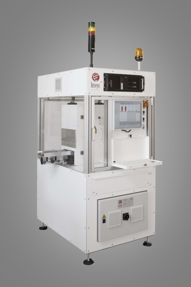
Wafer Inspection
Raise the efficiency of your production
Due to high added value in the production steps, it is important to guarantee frictionless operation and to avoid production shutdowns, particulary due to wafer breakage. Therefore, wafers with structural defects, e.g. cracks, saw marks or chippings should be detected and separated out.
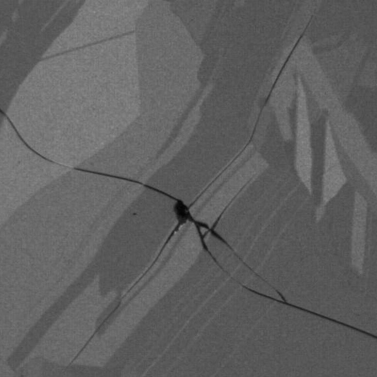
Microcrack detection
Our new technology is independent of the grain structure of multicrystalline wafers. Using illuminations and cameras in the IR spectral range results in the reliable detection of microcracks.
Laser structures
Solar wafers are structured with lasers to gain more efficiency. We have extensive experience measuring these structures to control the laser process and make sure that only correctly lasered wafers proceed to the next manufacturing steps.
Geometry
Providing lateral resolutions as small as 10 µm, the wafer geometry can be determined with high accuracy. Defects such as chippings can therefore be detected easily.
Topography
The topography on both sides can be determined with resolutions as small as 1 µm perpendicular to the wafer surface. It is thereby possible to detect small saw marks or chippings in addition to recording statistical data such as thickness or bending.
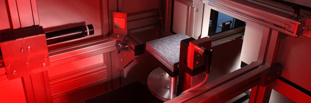
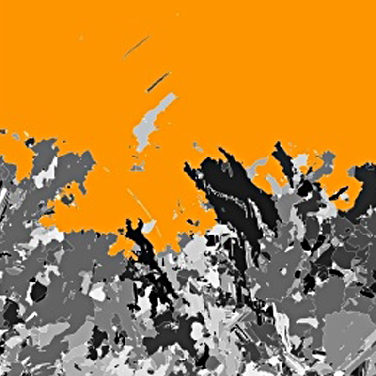
Grain analysis
Knowledge of the grain structure gives valuable information about the crystallization process. With the GEMINI tool the grain structure of each wafer can be characterized offline or inline for classification.
Your contact for wafer inspection

Andreas Eckl
+49 9131 61082-0
Contact