Semiconductor Inspection
Intego’s comprehensive portfolio of defect inspection, overlay and critical dimension metrology, as well as data analysis systems are specifically designed to support the semiconductor industry from initial product development to high volume manufacturing. Manual, semi-automated or fully-automated tool configurations are available for the quality assurance for front-end and back-end processes.
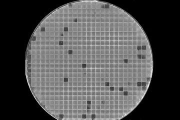
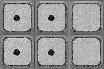
Typical inspection objectives are the detection of surface, material and process defects for bare, epitaxial, patterned and diced wafers. Both (semi) transparent and standard opaque wafers can be inspected with Intego’s systems. Inspection solutions for standard and advanced semiconductor materials like Si, SiC, GaN, GaAs, Ge as well as for device manufacturing processes of LED, OLED and MEMS can be offered.
The innovative modular tool concept allows a configuration of multiple inspection stages perfectly adapted according to customer's requirements. These innovative inspection systems combine many different inspection methods in just one tool and thus impress with a fascinating tool performance at high throughput and convincing cost of ownership. A continuous development of these systems including the wafer handling takes place in close cooperation with Intego’s customers.


