Halbleiter - Speziallösungen
Special Topics
Raise the efficiency of your production
The demand for customized optical inspection systems is constantly increasing. A new production process, a new product or the occurrence of a new type of defect often requires an adapted solution. For more than 20 years Intego has been developing customized wafer inspection and metrology systems for the front-end and back-end area in close cooperation with its customers. Requirements for throughput, handling, interfaces, SEMI conformity, and cost of ownership are considered in the same way during the development phase as the optical inspection technology, which is the heart of the system. In the end, the customer receives a customized inspection system that meets his requirements in the best possible way and thus makes a permanent contribution to improved product quality and productivity.
Special inspection topics are:
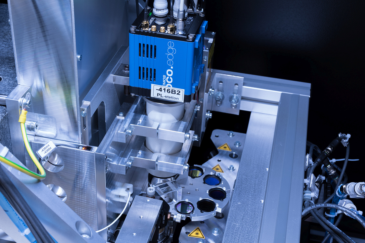
- UV to NIR photoluminescence (AQUILA PL): defect detection and material characterization in the field of opto- and power electronics (e.g. LED, SiC, GaN)
- Spectrometry: advanced crystal defect classification for power electronic materials
- Lifetime measurement (MODULUM): spatially resolved charge carrier lifetime measurements based on modulated luminescence
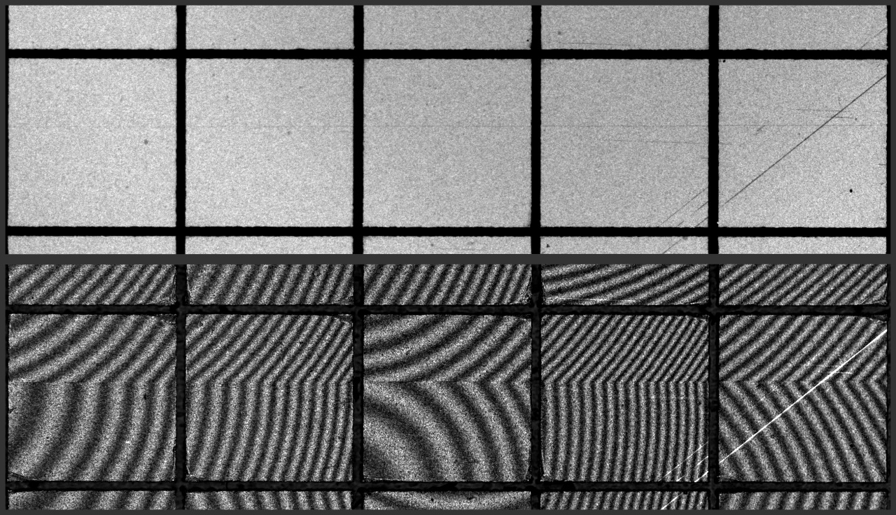
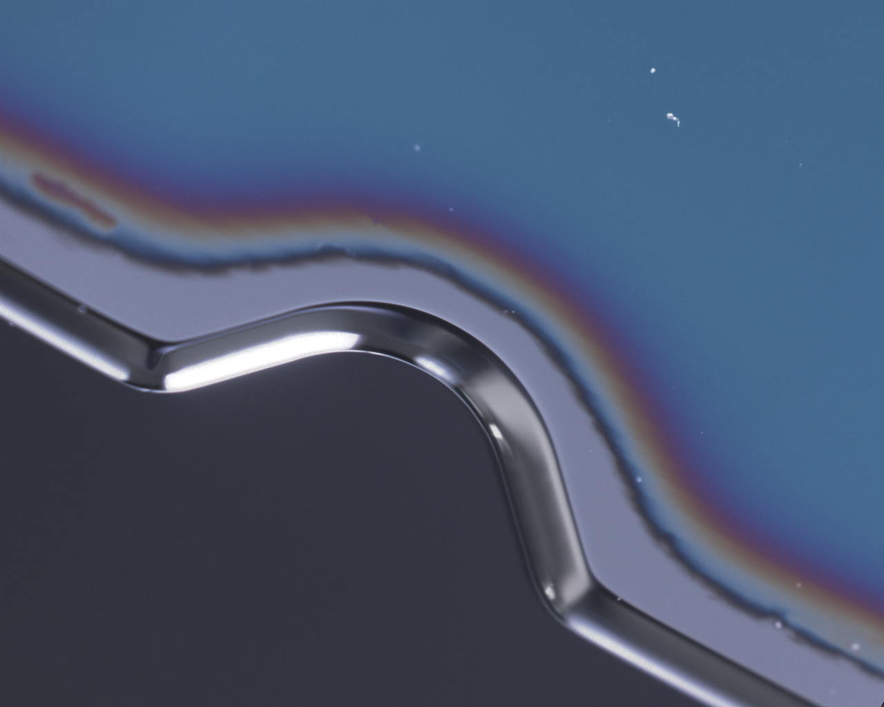
- Infrared inspection: fast and high-resolution microcrack detection in semiconductor and MEMS wafers
- Edge and notch inspection (LYNX): 100% wafer edge and notch inspection system using an unprecedented inspection concept
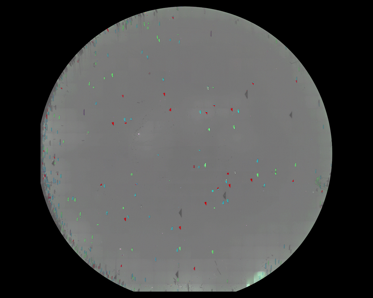
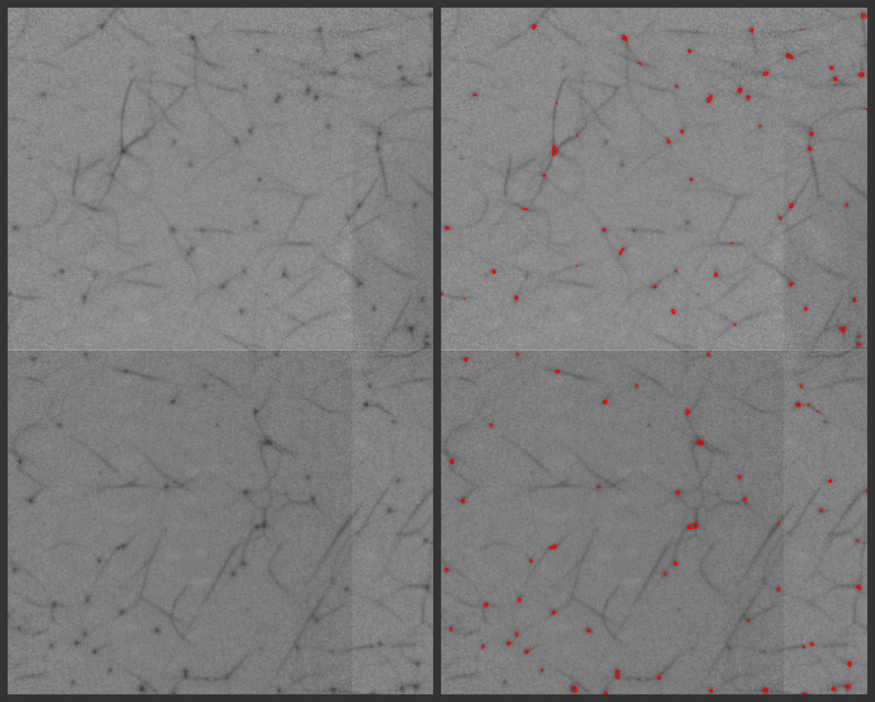
- Surface inspection: fast and sensitive surface inspection using laser scattering; reliable detection of particles down to 100 nm and smaller
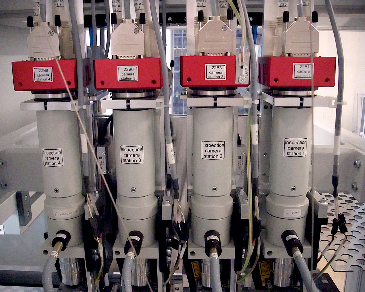
- Large and irregular shaped substrate and panel inspection: multi camera setups and customized handling solutions for the inspection of non-standard or oversized semiconductor substrates
- Microcrack detection: highly sensitive optical crack detection in diced wafers (e.g. LED, diodes, MEMS)
We are very pleased to announce that our activity for a photoluminescence based wafer inspection system was awarded the Semikron Innovation Award 2016 at the power electronics conference PCIM in Nuremberg. The official press release can be found here .
Some general performance data
Application
- customized and flexible hardware and software solutions for wafer and chip inspection
- inspection of opaque, partially transparent and transparent wafers
- system concepts for different wafer sizes and shapes (spectrum ranges from standard wafer sizes to 500 mm x 500 mm substrates)
Technology
- combination of several inspection and measurement methods in only one system
- simultaneous inspection with several focal planes, magnifications and illumination scenarios
- special inspection methods for improved image acquisition in case of uneven height distribution of the chips on the carrier film
- inspection by brightfield, darkfield, transmitted light, laser scattering, polarization, photoluminescence, interferometry, thermography, DIC, etc.
- customized illumination from UV to IR
- highest resolution measurement methods down to 0.2µm
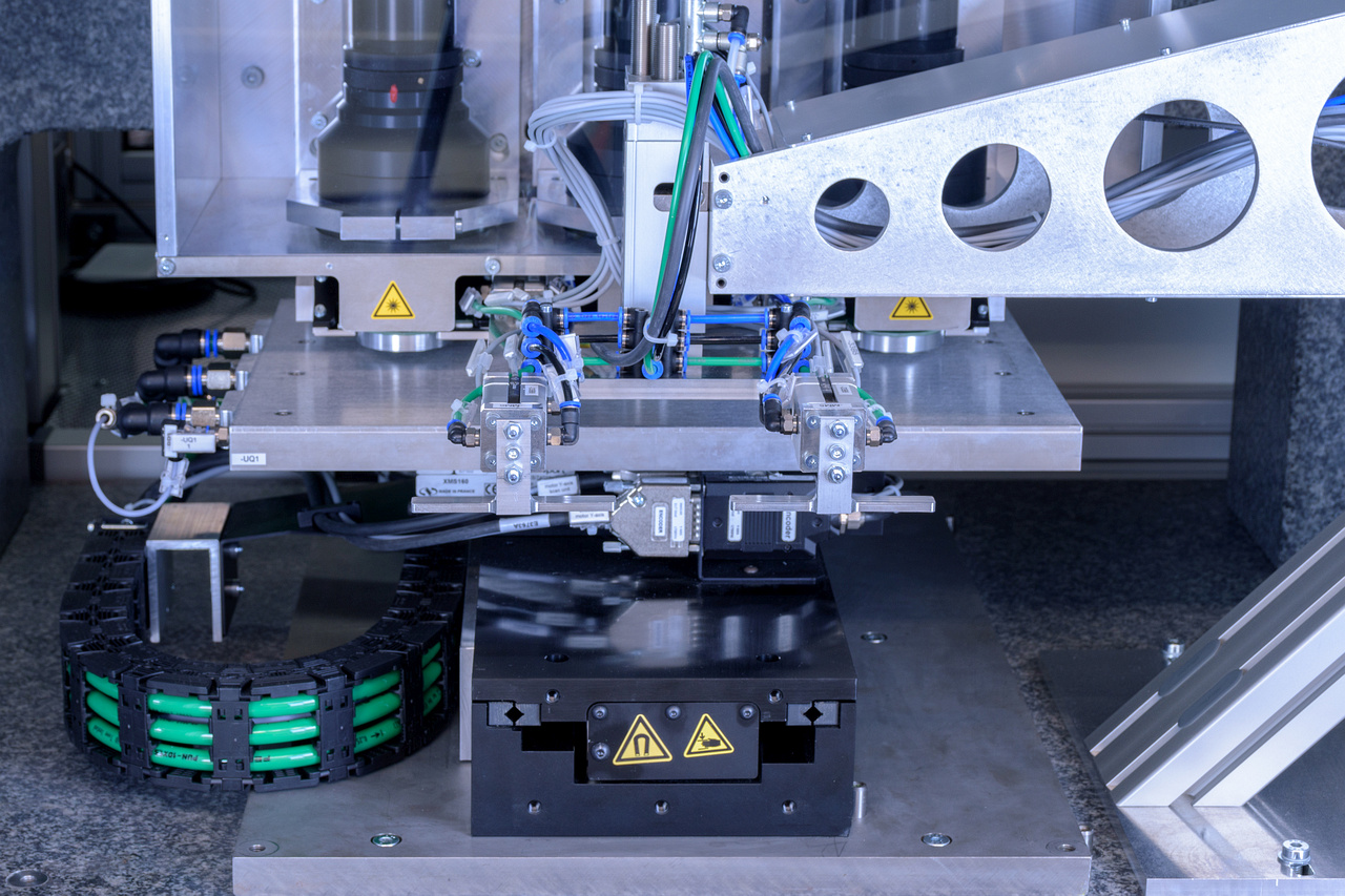
Wafer handling
- individual EFEM solutions or standard EFEM suppliers (e.g. Rorze, Brooks, InnoLas)
- customized chuck and end effector solutions
- special clean room and minienvironment solutions
Software
- advanced image processing algorithms based on state-of-the-art PC cluster solutions
- automatic chip inspection based on the Golden Samples principle or CAD information
- proprietary automatic defect detection and classification algorithms
- special pattern recognition or deep learning solutions
- comprehensive software for wafer defect analysis, result preparation and yield determination
- customized GUI, KLARF reporting and SQL database solutions
- SEMI software interfaces incl. SECS/GEM
Further options
If you require an individual solution, Intego offers free-of-charge feasibility studies based on sample parts. The prepared study will include a system design with draft specifications and a price estimate. Do not hesitate to contact us directly.
Your contact for special topics

Dr. Steffen Oppel
+49 9131 61082-0
Contact